Technology Overview
ALD technology Introduction
Atomic layer deposition (ALD) is a continuous thin film deposition technology based on vapor phase chemical processes. Most ALD reactions use two chemicals called precursors (also known as "reactants "). These precursors react sequentially with the material surface in a self-limiting manner. Targeting at the typical demand of market, ANAME provides comprehensive and mature ALD solution for relevant industrial partners. ALD is a chemical vapor deposition technique that was originally used to produce nanoscale insulating Al2O3 and zinc sulfide as a thin-film electroluminescent display (TFEL) material. ALD has the advantages of high precision, pinhole-free and high conformity nano-film deposition on various sizes and shapes of the substrate, therefore, it plays an indispensable role in the process of industrial production.

Process and film properties

Excellent adhesion
Chemical adsorption of the precursor onto the base material ensures excellent adhesion.

Saturated adsorption characteristics
The self-limiting nature of the surface reaction makes it possible to automate the process without the need for precise dose control and continuous operator intervention.

Ordered reaction
The ordered growth of the film provides extremely high film accuracy without in-situ feedback or operator intervention.

Surface controlled reaction
The surface reaction ensures the high conformity of the film under any condition, whether the substrate material is dense, porous, tubular, powdery or with other complex shapes.

Accuracy and repeatability
Per-cycle film thickness is determined by the process, but is usually 1A(0.1 nm).

Ultra-thin, dense and flat
ALD can deposit films less than 1 nm-thick. In some industrial applications, the film thickness is only 0.8 nm.

High productivity
Surface controlled growth characteristics make it possible to expand productivity by increasing batch size and substrate area.

Plasma-enhanced ALD
Films of some metals, low temperature oxides and nitrides can be prepared by using plasma during atomic layer deposition.

Roll-to-roll and continuous ALD
Roll-to-roll film deposition opens the door to many entirely new applications, such as the flexible electronics industry.

ALD for particles and powders
Combining conform coatings with granulated substrates creates a number of novel applications, such as altering the diffusion properties of battery materials.


ALD film material
The most common materials that can be deposited by atomic layers include (selected) :
Oxides: Al2O3, HfO2, SiO2, CaO, CuO, Er2O3, Ga2O3, La2O3, MgO, Nb2O5, Sc2O3, Ta2O5, TiO2, VXOY, Y2O3, Yb2O3, ZnO, ZrO2, etc.
Nitride: AlN, GaN, TaNX, TiAlN, TiNX, etc.
Carbides: TaC, TiC, etc.
Metals: Ir, Pd, Pt, Ru, etc. Sulfides: ZnS, SrS, etc. Fluoride: CaF2, LaF3, MgF2, SrF2, etc. Biomaterial: Ca10(PO4)6(OH)2(Hydroxyapatite) Polymer: PMDA - DAH, PMDA - ODA, etc. Doped nano-coatings and composite structures: ALD can realize a large number of different material combinations.
The application of ALD

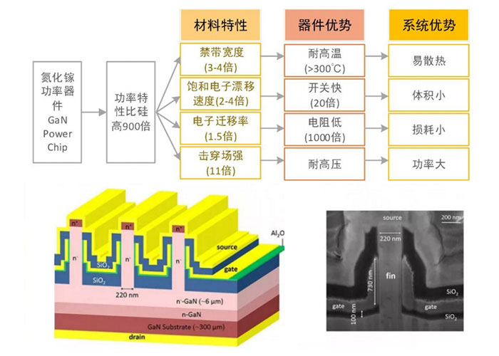
Power device ALD plays important roles in power devices. Among them, the film deposited by ALD process has controllable thickness, excellent replacement coverage. A number of high- breakdown voltage materials and devices include: GaN, SiC, traditional IGBT and other thin film materials, which involve the deposition of high-k dielectric film, including the deposition of gate insulation layer with low interface state. GaN GaN is widely used in chargers because of its high thermal conductivity and wide band gap, which can be adapted to small transformers and high power devices to achieve high efficiency charging effect. GaN films with controllable thickness can be deposited without damage by ALD method, so as to achieve the advantages of high efficiency in devices.

Radio Frequency Device (RF)
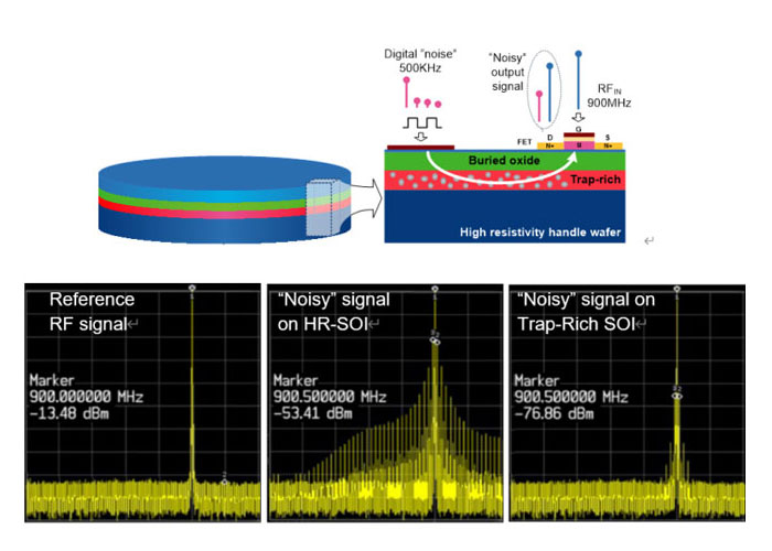
MOS and RFFE semiconductor devices using Group III-V materials in the periodic table requires metal oxide to realize a controllable layer of passivation. ALD process can be used to control the thickness of such surface passivation layer, and deposit high-dielectric-constant material stack to control the interface quality.

Ferroelectric storage
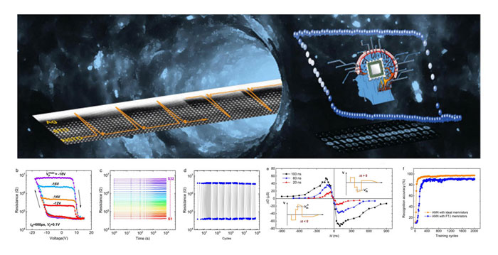
Ferroelectric material is a kind of material which has spontaneous polarization and this polarization can change under the action of external electric field. Therefore, ultra-thin ferroelectrics are of great significance for high density electronic devices, especially for FET and non-volatile memory. The existence of inversion symmetry failure and switchable electrical polarization in ultra-thin ferroelectric materials grown by low-temperature ALD was determined by the generation of second harmonics and advanced scanning probe technology, respectively. The efficiency and application range of ferroelectric storage are greatly improved.
Official account


